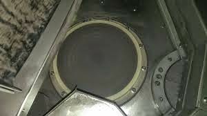
Tuesday, April 28, 2015

静电吸盘的基本构造和原理

静电吸盘的基本构造和原理

射频专家 发表于: 2007-4-04 04:31 来源: 半导体技术天地
静电吸盘的构造和原理对很多人来说都还是很陌生的。不妨在这儿开个头,慢慢再以对答方式把它解释透。

1。种类:基本分为两类。即库仑类和迥斯热背(JR或Johnsen-Rahbek)类。
2。两类吸盘都靠静电荷的同性相吸来固定硅片。
3。吸盘与晶片接触的表面有一层电介质。以前的吸盘用的电介质多为有机材料或阳极氧化层,现在已普遍采用陶瓷。纯电介质做成的吸盘为库仑类,参杂电介质做成的吸盘为迥斯热背类。
4。在吸盘的电介质层中镶嵌着一个直流电极(大小与硅片相当,稍小),用以接通到高压(低流)直流电源。
5。在没有等离子体的情况下,当直流电极被接通到高压(低流)直流电源后,电介质的表面会产生极化电荷(对库仑吸盘而言)。如果是迥斯热背类吸盘,电介质表面不仅有极化电荷,还有很大部分自由电荷,这是因为JR吸盘的电介质有一定导电性。电介质的表面电荷会产生电场,这一电场会进一步在置于吸盘之上的晶片表面产生极化电荷 (也可能包括部分自由电荷,取决于什么样的晶片及晶片表面是什么膜,有导电性或绝缘),分布在晶片背面的电荷与分布在吸盘上面的电荷极性相反,这样晶片解就吸盘吸住了。
6。 在没有等离子体的情况下,如果关掉被接通到直流电极(镶嵌在吸盘的电介质中)的高压(低流)直流电源,假若分布在晶片背面的电荷与分布在吸盘上面的电荷都是极化电荷,则晶片就被释放了,即吸力自动消失。
7。 在没有等离子体的情况下,假若分布在晶片背面的电荷与分布在吸盘上面的电荷中有一部分是自由电荷,  即使关掉被接通到直流电极(镶嵌在吸盘的电介质中)的高压(低流)直流电源,则晶片也不会完全被释放,即因残留电荷而仍存在一定的静电吸力。这种情况下,通常需要用反向的静电压来强制消除残留电荷,然后才能释放晶片。
8。在有等离子体的情况下,由于直流自偏压(self DC bias)的缘故,即使关掉被接通到直流电极(镶嵌在吸盘的电介质中)的高压(低流)直流电源,即在吸盘电压为零的情况下,晶片仍然会被吸盘·吸住。这是因为直流自偏压起到了吸盘电压的作用。在某些反应腔中(不是蚀刻机的),甚至不需要用高压(低流)直流电源的静电压,完全靠直流自偏压就足够完成吸住晶片的任务。所以,在处理完晶片后,需要一个释放菜单(dechucking recipe)来释放晶片,否则无法从反应腔中把晶片取出。
9。一般来说,迥斯热背类吸盘的吸力比库仑类的大。在对晶片温度控制要求很高的蚀刻机中,越来越多地采用迥斯热背类吸盘,其电介质通常是参杂的氮化铝陶瓷材料。氮化铝有很好的导热性。
10。晶片处理过程中,之所以需要把晶片牢牢地吸到吸盘表面,主要是增加晶片与吸盘之间的传热。此外,晶片背面与吸盘表面之间的氦气是传热的重要媒介。
11。在吸盘中,除了直流电极外,还有射频电极。射频电极用来提供晶片处理过程中需要的射频偏置功率。此外,吸盘中也需要冷却液的循环渠道和氦气的气道。其设计还是需要特别小心细致的。而且,它的设计受到别的方面的制约,如体积不能过大,否则会堵塞或降低反应腔的排气速度。

Ceramic Properties

Material Properties for Alumina Ceramics

Properties / MethodUnitPEC94PEC96PEC995PEC998
CompositionWeight %96% Al2O399.5% Al2O399.8% Al2O3
Process--SinteredSinteredSintered
Color--WhiteWhiteWhiteIvory
Densityg/cm33.693.713.903.92
Flexural Strength / MORMPa364372388395
Fracture Toughness, K(IC) Notched BeamMPa m1/24455
Hardness / Knoop 1000gKg/mm21200120014501500
Young’s ModulusGPa305305380380
Poisson’s Ratio--0.210.210.220.22
Average Grain SizeMicrons,10654
Max Use TemperatureDegrees °C1725172517251725
Thermal Shock Resistance, D°C300300250250
Gas Permeabilityatm-cc/secNoneNoneNoneNone
Dielectric Constant1 MHz, 25 °C9.19.29.810.5
Thermal Expansion Coefficient (25-1000oC)/°C7.8 x 10-67.8 x 10-68.0 x 10-68.0 x 10⁻⁶
Thermal ConductivityW/m·°K, 20°C22.524.929.030.0
Material Properties for Zirconia, Silicon Nitride, & EDM-Machinable Ceramics
Properties / MethodUnitTZ-30DTZ-30MSSN-310PEC EDM
CompositionWeight %YTZP Zirconia High StrengthMg-PSZ ZirconiaSilicon NitrideEDM Machinable
Process--Sintered & HIPPED*Sintered/ ToughenedSinter- Reaction BondedHot Pressed
Color--Varies (Gray-Green)IvoryBlackBlack
Densityg/cm36.055.833.203.90
Flexural Strength/ Four Point BendingMPa1400650800690>
Compressive Strength/ASTM-C773MPa, 25 °C25001750----
Fracture Toughness, K(IC)/SENB Notched BeamMPa m1/28105.8
Young’s Modulus/ Pulse-Echo MethodGPa220200310406
Average Grain SizeMicrons, m< 120--< 3
Max Use Temperature

Recommended Use Temp
Degrees °C

Degrees °C
1500

< 280
1500

< 1150
1600

up to 1600
1600

up to 1600
Thermal Shock Resistance,DT°C400400500--
Hardness / Knoop1000 gKg/mm21300120018002400
Dielectric Constant1 MHz, 25 °C28279--
Electrical ResistivityOhm-cm1013101310149 x 10-3
Thermal Expansion Coefficient
(25-1000 oC)
/°C10.3 x 10-610.1 x 10-63.1 x 10-67.0 x 10⁻⁶
Thermal ConductivityW/m·°K, 25°C2.22.22663

Sunday, April 26, 2015

Porous Ceramic

The generic word ‘filtration’ can encompass many applications across a wide range of industries, the majority of which can be served by the commonly available filter media where process temperatures are low and / or the environment inert.
It therefore takes a very special medium to tackle the difficult and unusual conditions found in today's chemical, petrochemical or general process industries.
These difficult problems were solved by  porous ceramic media that are chemically inert, stable and available in a variety of controlled and special grades, with temperature capabilities of up to 900ºC.

Available Ceramic Filter Media

We have a range of standard ceramic materials. Each has its unique characteristics and capabilities. The materials used most commonly are Pyrolith and Coralith.


Typical Filtration Tube Sizes
Various size,shape,pore size,porosity are available.

Flow Rates v Pressure Drop

Flow rate v pressure drop information can contact our sales rep.

Applications

Applications for filtration tubes fall into two main groups, each explained further on their own page:
  • Gas and Air Filtration
  • Liquid Filtration

Common Benefits

  • Controlled pore size
  • Controlled porosity and permeability
  • Coalescing capability
  • Chemically inert - can handle acidic gases
  • High Temperature capability to 900ºC
  • Range of standard element sizes
  • Low cost of ownership

Filter Cleaning

The cleaning properties of an element are dependent on the contaminate and the conditions. Normal methods of cleaning are surface brushing, back flushing or cleaning with a suitable solvent solution. With depth filter media, cleaning only usually removes surface contaminate with particles trapped in the pores being difficult to remove. Once the pressure drop across the filter reaches an unacceptable level, and cleaning has failed to restore the flow, then the filters should be replaced.

Saturday, April 25, 2015

Porous Ceramics

Thursday, April 23, 2015

Silicon Carbide (SiC) Polishing Disc

SiC Wafer Polishing Disc

  • Super flat  (1μm )
  • high thermal conductivity,
  • low thermal expansion coefficient 
  • porous or non porous


私の最大の光栄

私の最大の光栄は一度も失敗しないことではなく、倒れるごとに起きあがることにある。

www.chuck-table.com

Seguir caminando!

Mi mayor honor no es que no fallan ni una sola vez, es un objeto de levantarse cada vez que caen.


C'est la vie!

Friday, April 17, 2015

Porous Ceramic DISC

Porous Ceramic Disc 

(of Various pore size,porosity ,dimension and shapes)


Poröse Keramikscheiben unterschiedlicher Porengröße, Porosität, Dimension, sind Formen verfügbar

Disques céramiques poreuses de différentes tailles de pores, la porosité, la dimension, les formes sont disponibles

Discos cerámicos porosos de diversos tamaños de poro, la porosidad, la dimensión, formas están disponibles

さまざまな細孔径、気孔率、次元の多孔質セラミックディスクは、形状が可能です

Tuesday, April 14, 2015

wafer carrier


Keep walking with semi conductor industry with our ceramic know how

Keep Walking with Semi Conductor Industry with our ceramic know hows

Ceramic chuck table of 4inch,5inch,6inch,8inch,9inch,12inch


YOU WILL NEVER WALK ALONE!

CUSTOMERS & COMPETITORS,TOGETHER WE ARE MAKING THE WORLD BETTER!


Monday, April 13, 2015

Al2O3,S-Sic,ZrO2,Si3N4 Data Sheet

Main component99%Al2O3S-SiCZrO2Si3N4
Physical PropertyDensityg/cm33.903.163.2
Water Absorption%00.100.1
Sinter Temperature°C1700220015001800
Mechanical PropertyRockwell HardnessHV1700220013001400
Bend Strengthkgf/mm23500400090007000
Compression IntensityKgf/mm230000200002000023000
Thermal PropertyMaximum working temperature°C1500160013001400
thermal expansion coefficient 0-1000°C/°C8.0*10-64.1*10-6(0-500°C)9.5*10-62.0*10-6(0-500°C)
5.2*10-6(500-1000°C)4.0*10-6(500-1000°C)
Thermal Shock resistanceT(°C)200250300400-500
Thermal ConductivityW/m.k(25°C31100325
300°C)16100325
Electrical PropertyResisting rate of Volume◎.cm


20°C>1012106-108>1010>1011
100°C1012-1013-->1011
300°C>1012-->1011
Insulation Breakdown IntensityKV/mm18semiconductor917.7
Dielectric Constant (1 MHz)(E)10-297
Dielectric Dissipation(tg o)0.4*10-3---


Sunday, April 12, 2015

How to Attach Samples to Carrier Wafers for Plasma Etching or Deposition

The original link for this article is from 

 https://snf.stanford.edu/

How to Attach Samples to Carrier Wafers for Plasma Etching or Deposition

This folder contains procedures for attaching samples to carrier wafers in tools that require full wafer sizes. Pros and cons of each method are given. It should be noted that materials allowed in etch systems may not be allowed in depositions system. This is due to issues such as out-gassing (hazing of the deposited film) of the material or temperature of the system. Specific tool recommendations will be given.

Using Kapton Tape

Kapton tape, a commercial polyimide tape commonly found in the lab, can be used to attach pieces to a carrier wafer.

Using photoresist

Photoresist can be used to attach pieces to a carrier wafer. The commonly available resist in the lab may be used, 3612, SPR22-3 or -7. PMMA may also be used but it is described in another procedure page.

Using PMMA

This page describes two methods of using PMMA to attach samples to carrier wafers. A Wet Mounting procedure and a Heated Mounting procedure. These procedures are courtesy of labmembers Jim Kruger and Jan Petykiewicz.

Using Carbon Dots or Tape

Within is a description the the procedure using carbon dots or tape to attach small samples onto full wafers for etch or deposition in tools that require whole wafers. Included are hints and tips for greater success.

Using CrystalBond

This page describes the procedure for attaching smaller samples to larger of full wafer size carrier wafers.

Materials That are Unacceptable for Attaching Samples to Carrier Wafers

Here is a list of prohibited materials used in other labs or facilities that have been tried in SNF but rejected as not compatible with tools and processes. They are presented as informational only.

Labmembers Survey of Methods for Attaching Samples to Carrier Wafers

Labmember Ashish Pal asked the labmembers mail list for adhesive suggestions. Here are the results in summary.
Document