私の最大の光栄は一度も失敗しないことではなく、倒れるごとに起きあがることにある。
www.chuck-table.com
Seguir caminando!
Mi mayor honor no es que no fallan ni una sola vez, es un objeto de levantarse cada vez que caen.
C'est la vie!
Thursday, April 23, 2015

Friday, April 17, 2015
Porous Ceramic DISC
Porous Ceramic Disc
(of Various pore size,porosity ,dimension and shapes)


Poröse Keramikscheiben unterschiedlicher Porengröße, Porosität, Dimension, sind Formen verfügbar
Disques céramiques poreuses de différentes tailles de pores, la porosité, la dimension, les formes sont disponibles
Discos cerámicos porosos de diversos tamaños de poro, la porosidad, la dimensión, formas están disponibles
さまざまな細孔径、気孔率、次元の多孔質セラミックディスクは、形状が可能です
Disques céramiques poreuses de différentes tailles de pores, la porosité, la dimension, les formes sont disponibles
Discos cerámicos porosos de diversos tamaños de poro, la porosidad, la dimensión, formas están disponibles
さまざまな細孔径、気孔率、次元の多孔質セラミックディスクは、形状が可能です
Wednesday, April 15, 2015

Tuesday, April 14, 2015

Keep walking with semi conductor industry with our ceramic know how
Keep Walking with Semi Conductor Industry with our ceramic know hows
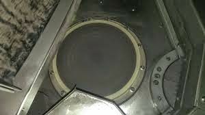
Ceramic chuck table of 4inch,5inch,6inch,8inch,9inch,12inch
Ceramic chuck table of 4inch,5inch,6inch,8inch,9inch,12inch


YOU WILL NEVER WALK ALONE!
CUSTOMERS & COMPETITORS,TOGETHER WE ARE MAKING THE WORLD BETTER!
Monday, April 13, 2015
Al2O3,S-Sic,ZrO2,Si3N4 Data Sheet
| Main component | 99%Al2O3 | S-SiC | ZrO2 | Si3N4 | ||
| Physical Property | Density | g/cm3 | 3.90 | 3.1 | 6 | 3.2 |
| Water Absorption | % | 0 | 0.1 | 0 | 0.1 | |
| Sinter Temperature | °C | 1700 | 2200 | 1500 | 1800 | |
| Mechanical Property | Rockwell Hardness | HV | 1700 | 2200 | 1300 | 1400 |
| Bend Strength | kgf/mm2 | 3500 | 4000 | 9000 | 7000 | |
| Compression Intensity | Kgf/mm2 | 30000 | 20000 | 20000 | 23000 | |
| Thermal Property | Maximum working temperature | °C | 1500 | 1600 | 1300 | 1400 |
| thermal expansion coefficient 0-1000°C | /°C | 8.0*10-6 | 4.1*10-6(0-500°C) | 9.5*10-6 | 2.0*10-6(0-500°C) | |
| 5.2*10-6(500-1000°C) | 4.0*10-6(500-1000°C) | |||||
| Thermal Shock resistance | T(°C) | 200 | 250 | 300 | 400-500 | |
| Thermal Conductivity | W/m.k(25°C | 31 | 100 | 3 | 25 | |
| 300°C) | 16 | 100 | 3 | 25 | ||
| Electrical Property | Resisting rate of Volume | ◎.cm | ||||
| 20°C | >1012 | 106-108 | >1010 | >1011 | ||
| 100°C | 1012-1013 | - | - | >1011 | ||
| 300°C | >1012 | - | - | >1011 | ||
| Insulation Breakdown Intensity | KV/mm | 18 | semiconductor | 9 | 17.7 | |
| Dielectric Constant (1 MHz) | (E) | 10 | - | 29 | 7 | |
| Dielectric Dissipation | (tg o) | 0.4*10-3 | - | - | - | |
Sunday, April 12, 2015
How to Attach Samples to Carrier Wafers for Plasma Etching or Deposition
The original link for this article is from
https://snf.stanford.edu/
How to Attach Samples to Carrier Wafers for Plasma Etching or Deposition
This folder contains procedures for attaching samples to carrier wafers in tools that require full wafer sizes. Pros and cons of each method are given. It should be noted that materials allowed in etch systems may not be allowed in depositions system. This is due to issues such as out-gassing (hazing of the deposited film) of the material or temperature of the system. Specific tool recommendations will be given.
Using Kapton Tape
Kapton tape, a commercial polyimide tape commonly found in the lab, can be used to attach pieces to a carrier wafer.
Using photoresist
Photoresist can be used to attach pieces to a carrier wafer. The commonly available resist in the lab may be used, 3612, SPR22-3 or -7. PMMA may also be used but it is described in another procedure page.
Using PMMA
This page describes two methods of using PMMA to attach samples to carrier wafers. A Wet Mounting procedure and a Heated Mounting procedure. These procedures are courtesy of labmembers Jim Kruger and Jan Petykiewicz.
Using Carbon Dots or Tape
Within is a description the the procedure using carbon dots or tape to attach small samples onto full wafers for etch or deposition in tools that require whole wafers. Included are hints and tips for greater success.
Using CrystalBond
This page describes the procedure for attaching smaller samples to larger of full wafer size carrier wafers.
Materials That are Unacceptable for Attaching Samples to Carrier Wafers
Here is a list of prohibited materials used in other labs or facilities that have been tried in SNF but rejected as not compatible with tools and processes. They are presented as informational only.
Labmembers Survey of Methods for Attaching Samples to Carrier Wafers
Labmember Ashish Pal asked the labmembers mail list for adhesive suggestions. Here are the results in summary.
Subscribe to:
Posts (Atom)